Construction
A semiconductor channel that allows current to flow between two terminals known as the source and drain is used to build a Junction Field Effect Transistor (JFET). Whether the device is an n-channel or p-channel JFET depends on the kind of semiconductor material utilized.
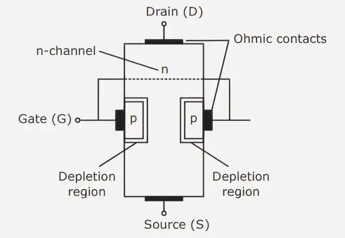
- A thin bar of n-type semiconductor serves as the channel in an n-channel JFET.
- The gate terminals are p-type regions that are dispersed on both sides of this channel.
- A single gate terminal is created by electrically connecting these p-type regions.
- The source and drain terminals are formed by connecting the ends of the n-type channel to metallic contacts.
- Similar to this, the gate of a p-channel JFET is formed by n-type regions, whereas the channel is composed of p-type material.
- To guarantee appropriate current flow, ohmic contacts are installed at the source and drain terminals.
- The p-n junction created by the gate-channel junction is essential for regulating the device's current flow.
Circuit Symbols
A JFET's three terminals are represented by its circuit symbol:
- Gate (G)
- Source (S)
- Drain (D)
The gate is connected to the channel by a line with an arrow, and the channel is typically depicted as a straight line. Below is the circuit symbols of n-Channel and p-Channel JFET
The JFET type is indicated by the arrow's direction:
- When the p-n junction is forward biased, the arrow in an n-channel JFET points in the direction of the channel, signifying the direction of conventional current.
- The arrow in a p-channel JFET points away from the channel.
- The gate is often depicted at the middle of the channel, reflecting the device's symmetrical design. Because of its symmetry, it is frequently possible to switch the source and drain terminals without having a major impact on functioning, particularly in basic analysis.
- The device boundary can alternatively be represented by enclosing the sign in a circle.
Unbiased JFET
When a JFET has no external voltage supplied across its terminals, it is said to be unbiased. The device is not entirely neutral on the inside, even in this state.
- Because the gate and channel produce p-n junctions, charge carrier diffusion causes depletion regions to spontaneously occur at these junctions. From both sides, these depletion zones stretch into the canal.
- The depletion region does not contribute to current conduction because it lacks free charge carriers.
- Consequently, even in the absence of external bias, the conducting channel's effective width is decreased.
- When voltages are supplied subsequently, this intrinsic depletion region is crucial to the JFET's functionality.
Working
A JFET operates by exploiting the electric field produced by the gate voltage to regulate the flow of current through the channel.
Current starts to move through the channel when a voltage is supplied between the drain and source terminals. The depletion region is wider because the gate-source connection is usually reverse biased.
When the reverse bias rises:
- The depletion zones extend farther into the channel.
- The path of effective conducting narrows.
- As a result, the drain current drops.
A JFET's basic working principle is to control current by changing the channel's width.
A higher negative voltage applied at the gate of an n-channel JFET increases the depletion region, which lowers the current. Applied voltages have the opposite polarity for a p-channel JFET.
Because the JFET controls current flow without requiring direct current at the gate, it can be used in applications with high input impedance.