In the RTL Design methodology, different types of registers, such as Counters, Shift Registers, SIPO (Serial In Parallel Out), and PISO (Parallel In Serial Out), are used as the basic building blocks for any Sequential Logic Circuits.
- Built using logic gates (AND, OR, NOT, etc.)
- Uses memory elements like flip-flops to store circuit state
The Synchronous Sequential Logic Design Process using a state diagram and its shortcomings are explained in the following example:
Let's say, we are to design a 2-bit synchronous Binary Up Counter whose count sequence is:
00 -> 01 -> 10 -> 11 -> 00 -> 01 -> ..... so on.- Step-1: In the 1st step, we draw a state diagram representing the above sequential circuit. The State Diagram representing the above counter is shown below:
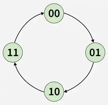
- Step-2: In the next step we derive the state table from the above given State Diagram The State Table is as given below:
Present State Q(n) Next State Q(n+1) Output 00 01 01 01 10 10 10 11 11 11 00 00 - Step-3: In the third step we need to choose the type of flip flop we will be using to store the state of the circuit, for simplicity, we will be considering the Positive Edge Triggered D-type Flip-Flop.We also need to determine the number of Flip-Flops required to represent the internal state of the circuit. The general formula for the number of Flip-Flops required:
Total Number of Flip-Flops =
Then we need to note down the Excitation Table for chosen Flip-Flop. The Excitation Table for the D-type Flip-Flop is shown below:\lceil log_2 N \rceil
Where,
N = Total Number of States in State TablePresent State Q(n) Next State Q(n+1) D X 0 0 X 1 1 - Step-4: In this step we combine the State Table from the 2nd step with the excitation table of the previous step as follows:
Q_A (n) Q_B (n) Q_A (n+1) Q_B (n+1) D_A D_B 0 0 0 1 0 1 0 1 1 0 1 0 1 0 1 1 1 1 1 1 0 0 0 0 - Step-5: Next, from the above table we try to express
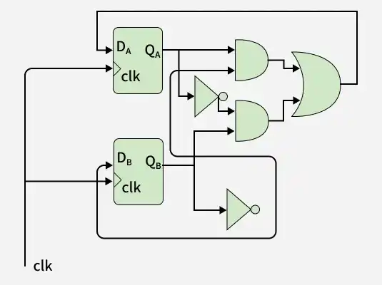
D_A, D_B as boolean functions ofQ_A (n), Q_B (n) . In this case the expression for bothD_A, D_B are trivial.D_A = Q_A \oplus Q_B \hspace{2.5cm} D_B = \overline Q_B - The Final Sequential Circuit is shown below:
Shortcomings of the above process:
- From the above example we observe that the Synchronous Sequential Logic Design process is a fairly involved process and requires us to go through a sequence of well defined steps even for simple circuits like the one above.
- Secondly, if the number of states become large then this process becomes cumbersome and time-consuming, and sometimes even impossible.
To Address the above drawbacks of the Sequential Logic Design process and to enable Digital Designers to design circuits of higher complexity with ease, the RTL design methodology was introduced. The most popular example of RTL Design is that of a Processor, which is nothing but a very sophisticated Finite State Machine with a very large number of states.
RTL Design vs Sequential Logic Design
| RTL Design | Sequential Logic Design |
|---|---|
| In RTL Design the basic building blocks are registers, Multiplexers, Adders. | In Sequential Logic Design the basic building blocks are the Logic Gates, Flip-Flops. |
| RTL Design is much closer to the Behavioural Design of a Logic Circuit as it models the data flow among different registers, and hence is much more intuitive. | Sequential Logic Design process is more mechanical in nature as compared to RTL design process |
| Finally, RTL Modelling allows us to synthesize complex circuits with a large number of States with much more ease as compared to Sequential Logic Design. | The Sequential Logic Design techniques are only applicable to circuits having a small number of states. |